



































































In the world of semiconductors, a long-standing mystery has puzzled scientists: Where do gallium vacancies go? Imagine trying to find a missing puzzle piece that has vanished before you even start searching! This is what scientists faced with gallium arsenide (GaAs), a material used in electronics. Despite predictions that these vacancies should be easy to spot, they always seemed to disappear without a trace—until now.
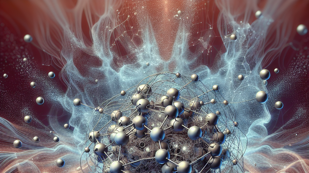
By introducing a fresh, multiscale method called Atomistically Informed Device Engineering (AIDE), researchers have made a groundbreaking discovery. They found that during the early stages of material impact, when energy is high, gallium vacancies quickly annihilate with other fast-moving atoms called arsenic interstitials. This pairing happens so swiftly, driven by an electric attraction, that the vacancies are effectively gone before we can even detect them with existing experimental methods.
Why should you care about this discovery? It paves the way for more reliable and efficient electronic devices by offering a deeper understanding of material behavior at the atomic level. Imagine your smartphone’s battery lasting longer or electronics that are less prone to overheating. By solving this gallium conundrum, this research could help design better, more durable tech in the future.
Did you know? Gallium arsenide is used in solar panels and LEDs due to its impressive ability to efficiently convert electricity into light.
FAQs
Why are gallium vacancies in semiconductors hard to detect?
Gallium vacancies in semiconductors are hard to detect because they are quickly neutralized by fast-moving arsenic interstitials before they can be observed using current experimental techniques.
What is the significance of discovering the behavior of gallium vacancies?
Discovering the behavior of gallium vacancies helps in understanding material behavior at the atomic level, paving the way for more efficient and reliable electronic devices.
How does the new AIDE method improve our understanding of semiconductors?
The new Atomistically Informed Device Engineering method improves our understanding by analyzing material changes at short time scales, revealing dynamic interactions that were previously inaccessible.
Can this research impact everyday technology?
Yes, this research could lead to the development of more reliable and efficient electronic devices, potentially improving the performance and durability of technology in everyday use.
Background
In semiconductor physics, vacancies refer to missing atoms in a crystal structure. Gallium arsenide (GaAs) is a compound used in electronics, where gallium atoms are sometimes missing, creating vacancies. These vacancies are expected to be detectable, but they have eluded observation due to their dynamic interactions with other atoms, such as arsenic interstitials, which can occupy the same space and effectively neutralize them.
History
For decades, researchers have studied gallium arsenide to improve semiconductor technology. Earlier studies focused on detecting static vacancies in these materials. However, despite predictions, gallium vacancies remained undetected, leaving a gap in understanding. This study uses a new multiscale approach, AIDE, to explore dynamic processes at short time scales, providing insights that were previously unattainable.
Based on “The case of the missing gallium vacancy in gallium arsenide: A multiscale explanation” by Leopoldo Diaz, Harold P. Hjalmarson, Jesse J. Lutz, Peter A. Schultz, available on arXiv (arxiv.org/abs/2504.15459), used under CC BY 4.0 (creativecommons.org/licenses/by/4.0/).